
Discrete DAC
|
Discrete DAC |
The Discrete DAC was built with the purpose of getting back to the basics of digital audio, away from the complicated silicon that tends to perform the digital to analogue conversion these days. The fundamental building block for the Discrete is an R-2R ladder network like this...
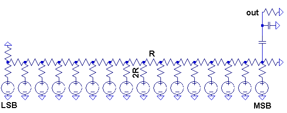
The sources/sinks for each bit are MOSFET switches. While it would be possible to create an entirely discrete design with no ICs at all, it is unlikely to yield much advantage. For reasons of cost and simplicity, standard 74HC-series logic is used to demultiplex the incoming I2S stream, and turn the wordclock strobe into pulses to change the switch states accordingly.
As the intention was to oversample the source 44.1kHz audio, more than 16 bits would be required in the ladder. 20 bits were implemented, as it was felt this covered the maximum resolution feasible from such a matrix board design. Inexpensive 1% metal film resistors were used, but were matched to a very high precision in order to improve linearity.
It is important to remember that any error in matching of the ladder will result in non-linearity. In order to keep a high level of linearity, it is required to take into account the switch Ron, as this affects the total 2R values seen by the ladder. Things are complicated by non-linearity of the switches according to temperature and current, and also that the resistance of the switch when sinking current may be different to the resistance for sourcing.
The easiest way to deal with switch Ron is by using a high ohmic trim resistor in parallel with the 2R position to reduce the effective 2R value to half of the R values, as desired. To save time and improve precision, a multi-turn pot in series with a large "base trim" resistor can be used to calibrate the ladder 2R positions, but the R positions must be as well-matched as feasible to each other in order to extract maximum resolution from the architecture.
To keep the design complexity down, a unipolar architecture was implemented, eliminating the need for separate positive and negative swing ladders. This requires the most significant bit (MSB) to be inverted, to add the offset to reproduce negative numbers - in this case, done by the transport.
Measured performance of the right channel - 1K sine wave at -3dBFS
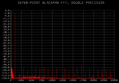
While the measured performance is underwhelming by modern standards, the subjective sound quality of the DAC is high. The main limiting factor in performance at the moment appears to be RFI - unsurprising, given the size of the matrix boards and the lack of a ground plane.
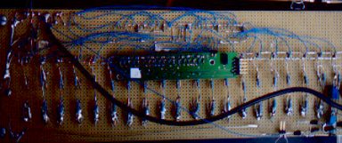
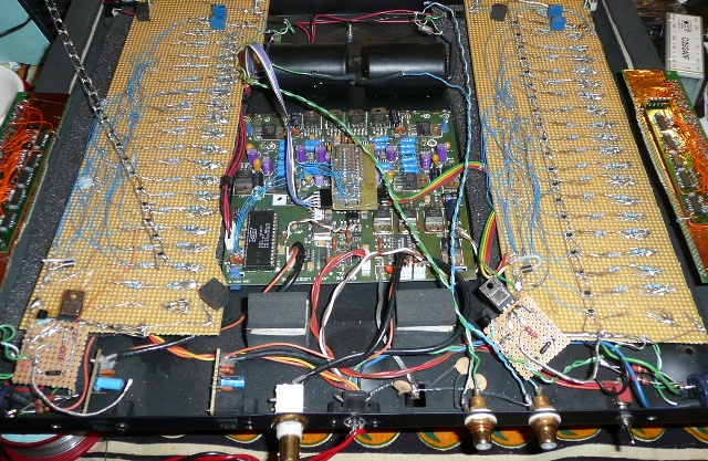
A double-sided printed circuit board has been developed, which is far more compact in size... as can be seen in the picture below...
The PCB version has the ladder reduced to 18 bits, as the matrix board version was unable to achieve 16 bit resolution using 47Kohm resistors, despite being tightly matched and trimmed - the Ron variation between buffers becoming very significant.
Another change is that the discrete logic buffers have been eliminated, as no significant crosstalk was found with driving directly from logic. A different logic family has been used to reduce Ron, which helps to compensate for the resistors being reduced to 22Kohm (done to provide better transformer compatibility without need for an output buffer).
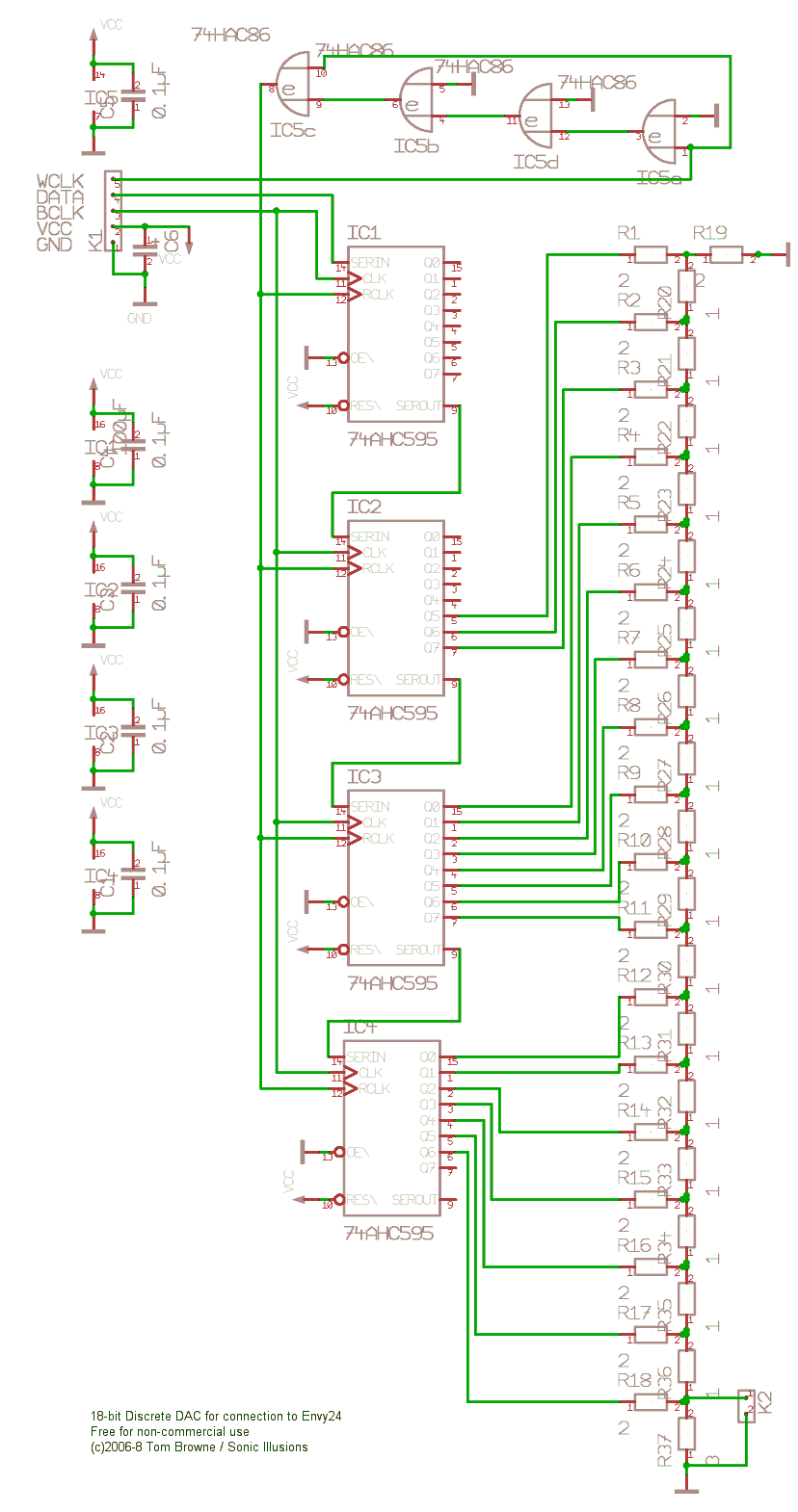
The schematic for the design can be downloaded here.
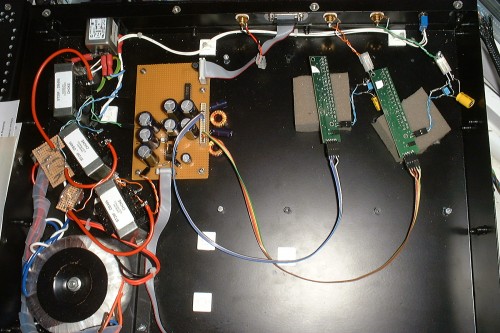
There is no active logic inside the box aside from that on the DAC boards themselves. All supply lines use LC filtering using very large chokes... various experimentation has been done with different circuits, from capacitance multipliers to direct battery drive.
Curiously, the lower impedance ladders seem to be more PSU dependent than the older high impedance ladders, whose subjective performance was mostly unaffected regardless of PSU quality.
The old design uses a simple 317 regulation chip with the adjust pin bypassed, followed by separate LC filters for each channel. This single regulator also provides power for one side of the I2S isolator cable. This design has since been modified to run off NiMH battery power which provides better isolation and a much more compact end result!
There have been a variety of Discrete DAC implementations, including an S/PDIF one... this used a Cambridge Audio IsoMagic as the donor base, with all the existing DAC and output circutry disabled...
There are three reasons why the IsoMagic makes an excellent base...
The first is that it uses the Pacific Microsonics PMD100 digital filter chip. I am of the opinion that most digital filter chips aren't very good (despite being better than what is built into most DACs), but this one is better than most off the shelf parts, and supports the required Complementary Offset Binary (COB) format that a unipolar Discrete DAC needs.
The second reason is that it supports clock locking with the partnering DiscMagic transport, where the clock is provided from the DAC and a divisor of it is fed back to the transport... this eliminates a lot of the jitter present in the S/PDIF connection link, and brings the quality much closer to an I2S link without the hassle of connection (the DAC will still work without the clock link with a regular S/PDIF source at lesser quality).
The third is that there's plenty of room to add extra circuitry, as can be seen in the picture above! The actual original Isomagic main PCB could be practically cut in half, as the DAC circuitry is all in the top half of the board... there are plenty of good quality components to scavenge for other projects... Oscons and polystyrene caps in particular.
The particular DAC boards shown in the picture above have been removed and are in the process of being modified for another design, but in order to have something that could appeal to DIYers, I developed a very simple single sided PCB which could be produced cheaply and be connected to the PMD100 very easily when put in COB 16-bit output mode. And here's the prototype...
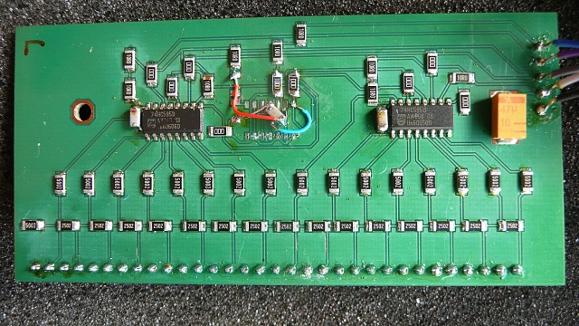
As can be seen, the prototype needed some "fine adjustments" to work correctly! These are to the wordclock in order to work correctly with the PMD100.
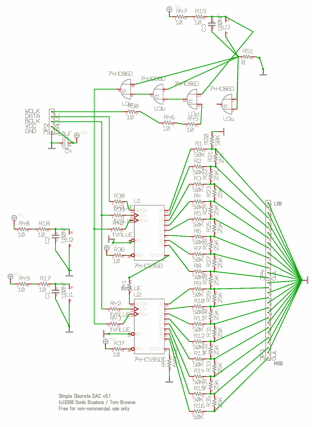
There is a corrected (but untested) schematic of the DAC downloadable from here. A PDF of the single sided PCB layout (again, untested) is here, and uses 0805 SMDs for the ladder side (the logic side is still 1206 for the link width). All the power pins should have a low DC resistance, so any link resistors should be either 0 ohm or bypassed with ferrites.
Three logic chips are used... two 595s and one 86. The 86 can be replaced with a single inverter gate if required (as in the prototype here) but I prefer to use the same chips across all the designs. As stated earlier, different logic families have different Ron values, which will affect the balancing of the ladder.
The design requires ladder resistors matched to at least 0.01%... these can be bought off the shelf, but it is cheaper to match by hand from 0.1% if you have the time and a suitably good multimeter of 6 or 7 digit precision! This also can allow you to do away with high ohmic trim resistors as you can compensate for the Ron by picking lower values for the 2R positions.
Generally if you are buying lower tolerance resistors it is a better idea to buy all one value (so, 50K, for example), and then parallel them to achieve half values, rather than buying 50K and 25K values... this makes it easier to get the matching required.